Application of Advanced ceramic Components in Semiconductor Manufacturing Processes
Semiconductor chips, as the core of electronic products, are widely used in various fields. In semiconductor manufacturing processes, precision ceramic components play important roles in key processes such as lithography, etching, deposition, chemical mechanical polishing (CMP), ion implantation, and wire bonding. This article provides an overview of the specific applications and advantages of advance ceramic components in these processes.
Applications in semiconductor manufacturing processes
| Materials | Applications |
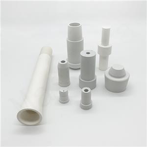
| Aluminum Oxide (Al2O3) | >Cavity components of semiconductor manufacturing >Polishing plates and platforms >wafer holders >Insulating flanges >End effectors |
| Silicon Carbide (SiC) | >XY platforms and bases >Focusing rings >Polishing plates >Wafer holders >Vacuum suction cups >End effectors >furnace tubes >boat-shaped carrier >cantilever paddles |
| Aluminum Nitride (AlN) | >Chip heaters >electrostatic clamps |
| Silicon Nitride (Si3N4) | >Semiconductor equipment platforms >Bearings |
<Lithography>
Photolithography is a fundamental process in semiconductor manufacturing that uses photosensitive  resist to create etch-resistant patterns on the processed surface. This process requires highly efficient, precise, and stable motion control and driving technologies, placing high demands on the dimensional accuracy and material performance of structural components.
Silicon carbide ceramics, known for their high elastic modulus and stiffness, resistance to deformation, high thermal conductivity, and low thermal expansion coefficient, are excellent structural materials used in key equipment for integrated circuit manufacturing, such as silicon carbide stages, guide rails, mirrors, ceramic chucks, and end effectors.
<Etching>
Etching is a critical step in semiconductor manufacturing processes. During the etching process in plasma etching equipment, the process chamber and internal components are subject to severe corrosion from high-density, high-energy plasma bombardment. This not only shortens the lifespan of the components but also generates volatile reaction byproducts and impurity particles inside the chamber, affecting chamber cleanliness.
Advanced ceramic materials with good corrosion resistance are widely used as plasma-resistant etching materials in wafer processing equipment. High-purity alumina coatings or alumina ceramics are commonly used as protective materials for etching chambers and internal components. Precision ceramic components used in plasma etching equipment include windows, viewports, gas distribution plates, nozzles, insulating rings, cover plates, focus rings, and electrostatic chucks.
<Deposition>

Deposition is a post-etching process and a core process in chip manufacturing known as "thin film deposition." Thin films are used to create conductive or insulating layers, anti-reflective coatings, and temporary etch stops. Different materials are used for different functions, requiring specific processes and equipment. Deposition processes can be categorized into physical processes (PVD) and chemical processes (CVD).
Similar to etching, thin film deposition processes involving plasma technology pose a risk of corrosion to the chamber and components. Therefore, advanced ceramics are used as materials for critical consumables in deposition equipment, including chamber lids, chamber liners, deposition rings, electrostatic chucks, heaters, electroplating insulators, and vacuum breaker filters.
<Chemical Mechanical Polishing (CMP)>
CMP is a crucial technology in semiconductor manufacturing processes, especially for sub-0.35μm processes, as it enables planarization and affects subsequent process yields. CMP combines mechanical friction with chemical etching. The working principle of CMP equipment leads to long-term friction and corrosion, causing wear and tear on critical consumables such as polishing tables, polishing pads, handling arms, and vacuum suction cups.
Alumina ceramics and silicon carbide ceramics possess properties such as high density, high hardness, high wear resistance, good heat resistance, excellent mechanical strength, and insulation properties at high temperatures. These properties make them ideal materials for critical consumables in CMP equipment.
<Ion Implantation>
Ion implantation is a mainstream doping technique in semiconductor fabrication, used to introduce impurities into active regions, substrates, and gate areas to increase conductivity. Ion implantation involves accelerating ions generated from an ion source and bombarding them onto the wafer surface. Bearings, vacuum suction cups, electrostatic chucks, and other ceramic precision components are commonly used in ion implantation processes.
<Wire Bonding>
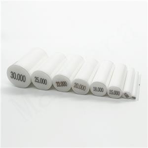
Wire bonding is a primary method used in semiconductor packaging to establish electrical connections between chips and substrates. Ceramic blades are essential tools in the wi re bonding process. Due to the high volume of wire bonding in a fully loaded wire bonding machine, ceramic blades are consumed at a significant rate. Currently, alumina is the primary material used for ceramic blades, and some manufacturers add zirconia to achieve a more uniform and dense microstructure, increasing density to 4.3 g/cm³ and reducing the frequency of wear and replacement of the blade tips during wire bonding.
In addition to the mentioned applications, precision ceramic components are also used in semiconductor equipment for processes such as oxidation, diffusion, and annealing in wafer thermal treatment devices. In summary, the application of precision ceramics in semiconductor equipment goes beyond our imagination, with numerous critical roles in various processes.
XIAMEN MASCERA TECHNOLOGY CO., LTD. is a reputable and reliable supplier specializing in manufacturing and sales of technical ceramic parts. We provide custom production and high precision machining for a wide series of high performance ceramic materials including alumina ceramic, zirconia ceramic, silicon nitride, silicon carbide, boron nitride, aluminum nitride and machinable glass ceramic. Currently, our ceramic parts can be found in many industries like mechanical, chemical, medical, semiconductor, vehicle, electronic, metallurgy etc. Our mission is to provide the best quality ceramic parts for global users and it is a big pleasure to see our ceramic parts work efficiently in customers' specific applications. We can cooperate on both prototype and mass production, welcome to contact us if you have demands.