Ceramic Substrate Series - The Benefits of Ceramic Substrate Grinding and Polishing
Surface grinding and polishing are often required for ceramic substrates prior to the metallization process, and this can be done on either a single or double-sided basis. This step provides three notable advantages:
Attaining finer patterns
By employing precise grinding and polishing techniques, ceramic substrates can achieve finer line patterns. This facilitates the design of more densely packed circuits with finer spacing and high-density interconnections. Controlling the flatness of the substrate greatly improves the transfer of mask patterns to the substrate surface, resulting in crisper lines and spatial details.
Enhancing top-bottom surface parallelism
Grinding and polishing the substrate improve the parallelism between the top and bottom surfaces, specifically the thickness tolerance of the substrate. This advantage allows for tighter control over the substrate's capacitance and inductance during the metallization and patterning processes. Since capacitance and inductance are crucial factors determining impedance, improving parallelism enhances the predictability and performance of RF and microwave circuits.
Achieving thinner metallization layers
Polishing reduces the amplitude of peaks and valleys on the substrate surface, enabling the use of extremely thin metallization layers. Thinner resistance layers increase the sheet resistance of the material, allowing for the formation of higher resistance values, particularly when utilizing serpentine patterns. This capability proves beneficial in meeting specific resistance requirements when employing thin-film techniques.
In summary, grinding and polishing ceramic substrates yield finer line patterns, improved top-bottom surface parallelism, and thinner metallization layers. These benefits contribute to enhanced circuit design capabilities, improved predictability, and enhanced performance in circuits.
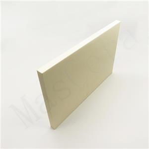
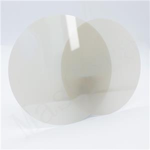
Mascera produces high-quality ceramic substrates using alumina, aluminum nitride, and silicon nitride as materials, and has introduced laser equipment on the production line for laser cutting, scribing, and drilling according to customer requirements. The size accuracy is high, the processing speed is fast, and the product stability is good. For surface treatment, polishing or DPC&DBC metallization can also be provided. If you want our quotation, please send us your design or requirement details.