Ceramic Substrate Series - Main processes for ceramic substrate metallization
Surface metallization of ceramics is an important step in the practical application of ceramic substrates in the field of electronic packaging. The wetting ability of metals on ceramic surfaces at high temperatures determines the bonding strength between metals and ceramics. Good bonding strength is an important guarantee for the stability of packaging performance. Therefore, how to implement metallization on ceramic surfaces and improve the bonding strength between the two is the focus of the ceramic substrate metallization process. The following describes several processes for ceramic substrate metallization.
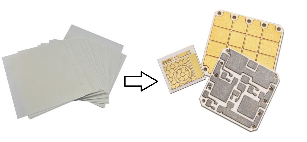
substrate metallization
1.Thick film method
Thic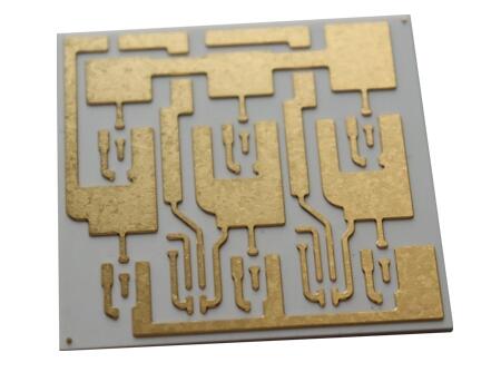 k Printing Ceramic Substrate (TPC) refers to the production process of using screen printing to directly apply conductive paste to the ceramic body, and then sintering at high temperatures to firmly attach the metal layer to the ceramic body. Depending on the viscosity of the metal paste and the size of the screen mesh, the thickness of the metal circuit layer is generally a film layer of several microns to tens of microns (increasing the thickness of the metal layer can be achieved through multiple screen printing).
Due to the limitations of the screen printing process, TPC substrates cannot achieve high-precision circuits. Therefore, TPC substrates are only used in electronic device packaging with low requirements for circuit accuracy. However, although thick film circuits have rough precision (minimum line width/spacing is generally greater than 100 μm), their advantages lie in reliable performance, low requirements for processing equipment and environment, high production efficiency, flexible design, small investment, and low cost. They are widely used in high voltage, high current, and high power applications.
Ceramic Substrate: The most commonly used substrate for thick film integrated circuits is 96% alumina ceramic. Although aluminum nitride ceramic also has good thermal conductivity, most metals do not have ideal wetting properties on aluminum nitride ceramics. Therefore, when using aluminum nitride as a substrate material, special process support is required. Common methods include: ① using glass material as a bonding phase to mechanically bond the metal layer to the AlN layer; ② adding substances that can react with AlN as a bonding phase to chemically bond with AlN.
2. Thin-film technology
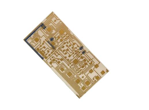
Thin-film technology (Thin Film Ceramic Substrate, TFC) is a method of preparing material film layers using techniques such as vapor deposition, photolithography, and etching. The term "thin-film" refers not only to the actual thickness of the film but also to the way the film is produced on the ceramic substrate. Thick-film technology is an "additive technology," while thin-film technology is a "subtractive technology." The use of photolithography and etching processes results in smaller feature sizes and clearer lines, making thin-film technology more suitable for high-density and high-frequency environments.
Thin-film circuits have thin lines (with a minimum line width of 2 μm) and high precision (with a line width error of 2 μm). However, due to the "small lines," they cannot tolerate fluctuations, so the surface quality of the substrate for thin-film circuits must be high. Therefore, the purity of the substrate used for thin-film circuits is high (commonly 99.6% purity alumina ceramic). Additionally, we know that high purity ceramics represent increased processing difficulty and cost. Furthermore, due to their small size, they present difficulties in application to high-power and high-current applications. Therefore, they are primarily used in low-current device packaging for the communication industry.
3.Direct plating copper
Direct plating copper (DPC) technology is a ceramic circuit processing technology that has been developed based on ceramic thin-film processing. Unlike traditional thick and thin film processing techniques, its processing is more focused on electrochemical processing requirements. After the ceramic surface is metallized by physical methods, conductive copper and functional film layers are electrochemically processed. Laser drilling (using lasers to cut and fill holes in DPC substrates) is used to achieve interconnection between the upper and lower surfaces of the ceramic substrate, thus meeting the requirements of three-dimensional packaging of electronic devices. The aperture is generally between 60 μm and 120 μm. The ceramic substrate is then cleaned using ultrasonic technology. A metal seed layer (Ti/Cu) is deposited on the surface of the ceramic substrate using magnetron sputtering technology, followed by the completion of the circuit layer through photolithography and development. Hole filling and thickening of metal circuit layers are achieved by electroplating, and the substrate's solderability and anti-oxidation properties are improved through surface treatment. Finally, the seed layer is removed by dry film stripping and etching, completing the substrate preparation.
Compared with other ceramic surface metallization methods, the DPC process has a low operating temperature, generally below 300°C, reducing manufacturing process costs, while effectively avoiding the adverse effects of high temperature on materials. The DPC substrate uses yellow light lithography technology to create graphic circuits with a controllable line width of 20-30 μm, a surface smoothness of below 3 μm, and a graphic accuracy error controlled within ±1%, making it very suitable for electronic device packaging with high circuit accuracy requirements. Its drawbacks are the limited thickness of the electroplated copper layer, significant pollution caused by electroplating wastewater, and a slightly lower bond strength between the metal layer and the ceramic.
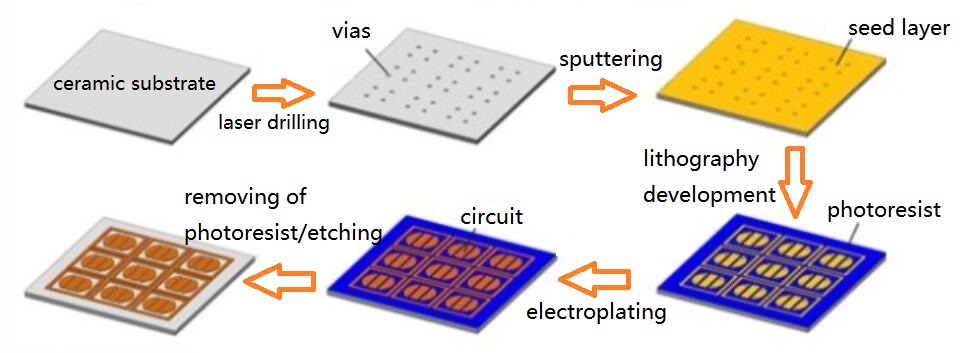
Preparation process for DPC ceramic substrate
4. Direct Bonded Copper (DBC)
Direct Copper Bonding (DBC), also known as Direct Bonded Copper Ceramic Substrate (DBC), is a metallization method that directly bonds copper foil onto the surface of ceramic substrates (mainly Al2O3 and AlN). The basic principle is to introduce oxygen into the interface between copper and ceramics, and then form a Cu/O eutectic liquid phase at 1065~1083℃, which reacts with the ceramic base and copper foil to generate CuAlO2 or Cu(AlO2)2, and achieves bonding between the copper foil and the substrate with the help of the intermediate phase. Since AlN is a non-oxide ceramic, the key to depositing copper on its surface is to form a transition layer of Al2O3, which helps to achieve effective bonding between the copper foil and the ceramic substrate. The copper foil used in DBC hot-press bonding is generally thick, ranging from 100 to 600μm, and has strong current-carrying capacity, making it suitable for device sealing applications in extreme environments such as high temperature and high current. It is a well-established standard device in the field of IGBT and LD packaging, but the minimum line width on DBC surfaces is generally greater than 100μm, making it unsuitable for the production of fine circuits.

Preparation process for DBC ceramic substrate
5.Active Metal Brazing (AMB) Ceramic Substrate
Due to the high preparation temperature and large interface stress of DBC ceramic substrates, Active Metal Brazing (AMB) ceramic substrates are an upgraded version of DBC. A small amount of active elements (such as Ti, Zr, Hf, V, Nb, or Ta rare earth elements) are added to the metal solder to significantly reduce the bonding temperature between the copper foil and the ceramic substrate.
AMB substrates rely on the chemical reaction between the active solder and the ceramic to achieve bonding, so their bonding strength is high and their reliability is good. However, this method is more expensive, suitable active solders are limited, and the composition and process of the solder have a significant impact on the welding quality.
6.Co-Firing
Multi-layer ceramic substrates using thick film technology to embed passive components such as signal lines and microfine lines into the substrate can meet many requirements of integrated circuits, and have received wide attention in recent years.
There are two types of co-firing: High Temperature Co-Firing (HTCC) and Low Temperature Co-Firing (LTCC). Although the process flow of the two types of co-firing is basically the same, the sintering temperature is significantly different. The main production process includes slurry preparation, tape casting, drying, drilling via holes, screen printing filling, screen printing circuitry, laminating sintering, and final slicing and other post-processing processes.

