precision ceramic components are the foundation of the semiconductor industry
As a key component of semiconductor production equipment, the R&D and production of precision ceramic components directly affects the development of the semiconductor equipment manufacturing industry and even the entire semiconductor industry chain. It can be said that precision ceramic components are the foundation of the entire semiconductor industry.
The semiconductor equipment market will exceed 100 billion US dollars, and ceramic components account for more than 10% of the cost
Recently, the Semiconductor Industry Association (SIA) said that global chip sales in 2021 will reach a record $555.9 billion, an increase of 26.2% over the previous year. The association expects global chip sales to grow 8.8% in 2022 as chipmakers continue to expand capacity to meet demand.
The rapid development of the semiconductor market has brought the upstream equipment market.
It is understood that wafer fab equipment spending is expected to continue to grow in 2022, following a year-on-year increase of 17% in 2020 and a year-on-year increase of 39% in 2021. SEMI (International Semiconductor Industry Association) pointed out that in 2022, the global front-end wafer fab equipment (excluding front-end process equipment for packaging and testing, generally wafer manufacturing equipment) expenditure is expected to exceed 98 billion US dollars, reaching a record high, the third consecutive year of growth.

Precision ceramics have become a key component of semiconductor equipment, accounting for more than 10% of the cost.
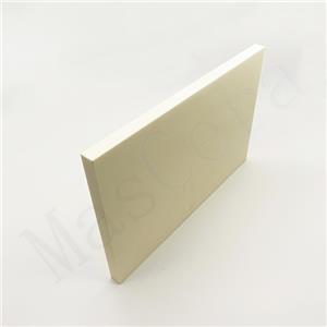
In high-end lithography machines, in order to achieve high process accuracy, ceramic parts with good functional composite, structural stability, thermal stability, and dimensional accuracy need to be widely used, such as E-chuck, Vacumm-chuck, Block, magnetic Steel skeleton water-cooled plates, mirrors, guide rails, etc., these key components are generally made of precision ceramic materials.
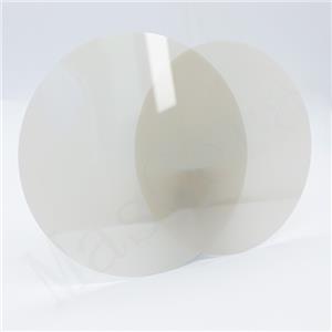
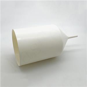
In the etching equipment, the chamber material of the etching machine is the main source of wafer contamination, and the degree of influence of plasma etching on it determines the yield, quality, stability of the etching process, etc. of the wafer. Therefore, researching and developing an extremely etch-resistant cavity material has become a very challenging task in the semiconductor integration industry and plasma etching technology. At present, high-purity Al2O3 coatings or Al2O3 ceramics are mainly used as protective materials for etching the cavity and the components in the cavity. In addition to the cavity, the gas nozzle of the plasma equipment, the gas distribution plate and the fixing ring for fixing the wafer also require precision ceramics.

A semiconductor device seems to be made of metal and plastic, but in fact, there are many high-tech precision ceramic components hidden inside. In short, the application of precision ceramics in semiconductor equipment is far more than we think
Mascera Technology is a professional supplier for technical ceramic parts coming from China, we are focusing on providing ceramic parts in excellent properties, high accuracy, constant quality and competitive cost. We offer tailor-made production as per customers' request on ceramic materials of Alumina Ceramics (Al2O3), Zirconia Ceramic(ZrO2), Boron Nitride Ceramics(HBN&PBN), Silicon Nitride Ceramics (Si3N4), Silicon Carbide Ceramics (SiC), Aluminum Nitride Ceramics (AlN) and Machinable Glass Ceramics. Any related demand about technical ceramics, please contact us, we will do our best effort to solve your problem.